Monolith pinout search guide
Description
This article was planned as a short guide for monolith pinout research. The main idea of this article is not to study step-by-step how to search pinout in all possible cases, but to understand the main principle and main idea of this process which is rather complicated and required a lot of experience. In other words – this article is posted “as it is”. We don’t want to say that the current example is the best one, and all tools and hints that we are describing would be the best choiсe in the world. Exist a lot of methods, and we are going to share only one of them.
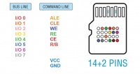
PC-3000 products are produced for data recovery, but monolith pinout research is an additional branch (rather large by the way) which is not contact with our technology directly. It’s the additional market, with its own “underwater rocks”, problems and profits. That’s why we provide only overview information, for better understanding and realizing “Do I really want to spend my life for dealing with this pinout research or not?”
So, where should we start? Of course – from
Equipment preparing
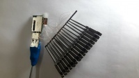
In our article, we will start our research line from the point where we will use healthy monolith. Of course, sometimes we can try to find pinout even if we have only damaged monolith. But this process would be more complicated, and sometimes it will not provide any result after a long time of attempts to get it. Why should we use healthy donor monolith? Because for detecting some bus lines and command lines, we should make writing operations on monolith. And of course, in case of real corruption, all writing operations would be impossible to make with damaged monolith. So, here are 3 main things that we should have before starting - see attached(pic.2)

If you don’t have patience – better even not to start this process at all. You will save your time and your nerves.
Ok, what about other equipment? Let's see…(pic.3)
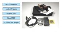
Healthy Monolith with the same pinout, as our damaged monolith have.
We should find exactly the same model, with the same capacity and brand, which have the same technological pinout on the bottom side of the chip;
Logical Analyser
If you can buy a good Logical Analyser with the price of 6000-10000$ – it would be perfect. But for beginners we recommend to use PC-Based Logical Analysers with the price of 500-1000$. We can recommend:
- АКИП-9102 – Russian Model with 32 channels and 200MHz Frequency. It also contains ENGLISH menu and it’s convenient to use even for foreign customers;
- GoodWill GLA-1032 – the same twin-brother to АКИП-9102 with 32 channels, 200MHz Frequency and almost the same interface.
- Actually, you can buy any logical analyzer that you want. The main terms – it should have at least 32 channels and support 200MHz Frequency.
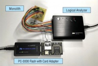
In our example we will use PC-3000 Flash with Card Adapter, but in real life you can use a common Card Reader. The only thing – it would be more complicated to control the power supply on on it. Sometimes we will need to switch it ON/OFF;
Circuit PCB
actually, it’s just a specific board for more convenient soldering wires on MicroSD. You can try to find similar boards in Aliexpress or in Amazon;
ONFI documentation
ONFI documentation with description of NAND signals (pretty useful for our task!).
STEP 1. Goals and first connection
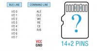
What we are looking for? We are trying to find all technological outputs signals, which will help us to find pinout. In our example, we will take a common MicroSD card with 8-bit bus line. Finally, we should find the following contacts(pic.4):
Usually, VCC and GND are not required to be found on technological pins. You can just use a default Monolith interface for providing the power supply. But of course, sometimes GND and VCC pins could be also found on technological pinouts, and we recommend to check all pins and found GND and VCC on pin map too. It will help us to detect pins that we should exclude from research.
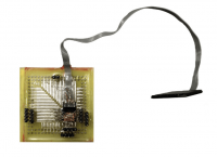
Let's prepare our monolith. As we told before, it’s a MicroSD card which we are going to solder to special Circuit PCB for convenient working process. We should solder wires to all targeting pins (excluding VCC and GND). The main idea of this preparation – Monolith should be soldered through techno pins + should be connected with SD or microSD interface. In our example we put microSD to SD adapter for making reading and writing operations on it(pic.5)
But construction of soldering might be different. It’s only example(pic.6) Finally, we should plug all Digital Logical Analyser contacts to our Monolith, and prepare everything like this: (pic.7)
STEP 2. Logical Analyser Interface and steps of Monolith initialization
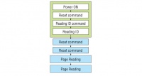
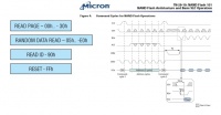
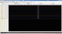
First of all we should remember, that every time when we starting the power supply on healthy monolith, it makes some steps for reaching it initialization status. Here is the example of commands which are going to be sent on monolith after power supply (pic.8,9)
With the help of documentation, we can try to detect how our lines will be changed after power supply. We can compare signals from Logical Analyser with our documentation schemes, and finally – find their values.
Here is the main screen of АКИП-9102 Logical Analyser software. We found that from 24 lines, 8 – are connected to GND, VCC or not changing their status after POWER ON. That’s why we leave only 16 of them – those lines, which are changing their values. Settings of LA you can see on pic.10
Also, please note that PC-based Logical Analysers (further – LA) doesn’t have enough RAM for showing you changes by all lines in real time. That’s why during first 5-10 seconds after power supply, LA make a snapshot (it situated below in the screen) that will allow us to move along it, change the scale and see how lines are changing.
STEP 3. Pinout Research. Command Line


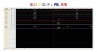


Using documentation for NAND signals we know that the first 4 contacts which makes a small jump after Power Supply – CE, RE, R/B, WE. Right now we don’t know where are exactly each of them, but at least we know that those 4 lines – are our the targets.
Next, lets try to detect where our BUS Group and WE, R/B are situated. Using the following scheme, we will detect where all of them are situated. We know that all lines in I/Ox (Bus line) should goes UP, when WE goes down. After some tome, R/B also should goes down. Lets see:
Then, lets try to find CLE, ALE and RE using the same algorithm:
CLE goes UP when WE goes DOWN:
ALE goes UP when WE goes DOWN, some time after CLE:
RE goes UP-DOWN, UP-DOWN, UP-DOWN:
Finally, we know WE, R/B and RE. Now, we can detect CE if we will return back on the first screen:
Now, all command lines are found. Next step would be – searching for the Bus Lines.
STEP 4. BUS line detection
Bus line detection would be the most complicated step, because for most cases we have to write bytes on monolith and read them to detect which lines are changing. But in our example we will describe another way which is not required any writing operations.
Lets check our monolith more detail. We know that manufacture is Toshiba, and capacity of this chip is 8GB. Using information about chip ID, we can try to imagine what is the first two bytes should be in our monolith:
Then, lets try to find how our lines in BUS area are changing:
f course in our example we put all BUS lines together, one by one. In real case they would be mixed. But this information will help you to detect how to find group of lines and how to detect all I/O lines.
Finally, we can say that pinout has been found. And now we can try to start solder wires to real monolith, and read it content in DUMP file 🙂